
Prediction of the atomic structure and thermoelectric performance for semiconducting Ge1Sb6Te10 from DFT calculations
 0
0Abstract
Pseudobinary alloys (GeTe)m(Sb2Te3)n (GST), known as the most popular phase change materials for data-storage applications, also exhibit great potential as thermoelectric (TE) materials due to their intrinsically low lattice thermal conductivity (κl) and high electrical conductivity. Among the GST compounds, the Sb2Te3-rich Ge1Sb6Te10 (m = 1 and n = 3) crystallizes into a complex trigonal structure with a 51-layer long period stacked along the c-axis, which may generate various possible atomic arrangements, thereby affecting the electronic and transport properties. Here, using ab initio calculations, we demonstrate that, besides the two experimentally known atomic sequences (GST-I and GST-III), Ge1Sb6Te10 has two novel stable stacking configurations (GST-II and GST-IV). GST-IV exhibits semi-metallic behavior, whereas GST-I and GST-II are semiconductors. Both semiconducting stackings have low κl of 0.86 and 0.78 Wm-1K-1 at 300 K, owing to their small phonon group velocities and short phonon lifetimes. Moreover, they show a combination of high n-type Seebeck coefficient and electrical conductivity due to the steep slope of conduction band density of states near bandgap, multiple conduction pocket electrons, and multiband conduction. The maximum ZT values of 2.23 and 1.91 are achieved in n-type stackings GST-I and GST-II at 710 K. Our work sheds light on the great potential of Ge1Sb6Te10 with different atomic stackings for TE applications and will stimulate further experimental study. More importantly, from the perspective of materials informatics, this study provides significant insights that crystal systems with multilayered structures may open a viable route for creating new functional materials.
Keywords
Introduction
The pseudobinary chalcogenides (GeTe)m(Sb2Te3)n (GST) with m, n = integer are well-known as excellent phase change materials for nonvolatile memory devices due to their fast and reversible phase transition between crystalline and amorphous states[1,2]. Besides the applications in information storage, GST compounds are also expected to be potential thermoelectric (TE) materials because of their intrinsically low lattice thermal conductivity (κl) and relatively large electrical conductivity (σ)[3-5]. Specifically, these two properties are beneficial to enhance the dimensionless figure of merit ZT = S2σT/(κl + κe) (where S is the Seebeck coefficient and κe is the electronic thermal conductivity), which characterizes the performance of a TE material. In recent years, many studies on GST alloys have indeed focused on their TE performance[6-12]. For example, the ZT value of bulk GeTe-rich GST compound is as high as 1.3 at 723 K[7]. More recently, it has been reported that maximum ZT (ZTmax) values of 0.4-0.6 were achieved at 750 K for three undoped quasi-two-dimensional GST systems (Ge2Sb2Te5, Ge1Sb2Te4, and Ge1Sb4Te7)[9]. The In-substituted hexagonal Ge2Sb2Te5 (i.e., Ge1.85In0.15Sb2Te5) gives the ZTmax of 0.78 at 700 K, a ~2-fold improvement compared with the undoped system[8].
Despite the wide investigations of GST materials, however, the detailed atomic structures of the stable phase for many GST compositions have not yet been clarified, owing to their complex multilayered structures. For many GST compositions (e.g., Ge2Sb2Te5, Ge1Sb2Te4, Ge1Sb4Te7, and Ge3Sb2Te6), there is more than one proposed atomic stacking sequence considering the atomic positions of Ge and Sb[13-16], thereby affecting their performance. In particular, it has been proposed that one of the stable atomic stackings of hexagonal Ge2Sb2Te5 is a topological insulator while the other is not at ambient condition[17,18]. Moreover, we previously demonstrated that the atomic arrangements have great effects on the electronic, mechanical, and vibrational properties of layered GST systems[16,19,20]. Besides, their lattice thermal conductivity and electrical transport properties show a significant dependence on the atomic stacking, thus resulting in differences in thermoelectric performance[10,21]. These facts suggest that understanding the structural arrangement of stable GST compounds is essential for their technological applications.
Among the GST alloys, crystalline Ge1Sb6Te10, which contains rich Sb2Te3 units (i.e., n = 3), adopts a very complicated multilayered trigonal symmetry (R̅3m, No. 166) with 51 atomic layers (within a unit cell) stacked along the c-axis via van der Waals (vdW) forces between Te-Te layers[22,23]. Such a complex structure with a very long layer period renders Ge1Sb6Te10 a promising TE material[24,25] and offers great possibilities to explore its atomic stacking-polymorphs. Therefore, to get insights into the atomic stacking structures of Ge1Sb6Te10 and the corresponding effects on electronic and transport properties, we start our investigations from seven possible atomic arrangements [the inset of Figure 1, and Supplementary Figure 1 and Supplementary Figure 2 of Supplementary Material (SM)]. Using ab initio density functional theory (DFT) calculations, we first examine their structural stability. In addition to the two experimentally documented atomic stackings (GST-I[22] and GST-III[23]), two types of novel state configurations, GST-II and GST-IV, are successfully identified. Then, we study the electronic structures of stackings GST-I, GST-II, and GST-IV and find that they vary between semimetal (GST-IV) and semiconductor (GST-I and GST-II). Finally, we focus on the transport properties and thermoelectric performance of semiconducting GST-I and GST-II. The results show that the lattice thermal conductivities of both stackings are below 1 Wm-1K-1 at room temperature, which is attributed to their low phonon group velocities and short phonon lifetimes. In addition, they exhibit high n-type power factors, resulting from the large Seebeck coefficients and high electrical conductivities. Owing to the favorable thermal and electrical transport properties, the ZTmax values of n-type GST-I and GST-II reach up to 2.23 and 1.91 at 710 K, suggesting their great promise as medium-temperature TE materials. Our work sheds light on the great potential of Ge1Sb6Te10 with different atomic stackings for TE applications and will stimulate further experimental study.
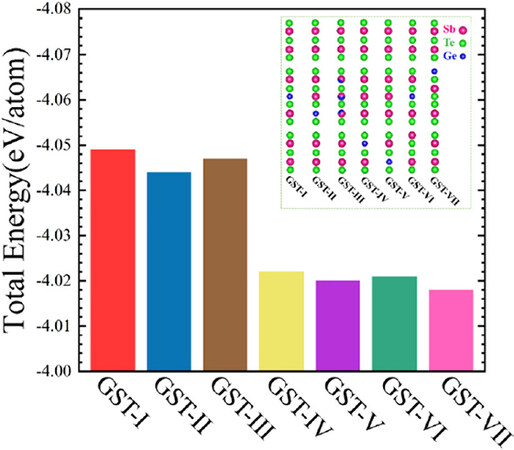
Figure 1. Calculated total energy for the seven atomic stackings of Ge1Sb6Te10. The inset corresponds to the basic stacking units with 17 atomic layers of each configuration.
Materials and methods
Ab initio calculations were performed within the framework of DFT using the Vienna ab initio simulation package (VASP)[26]. All theoretical calculations in this work were carried out automatically and intelligently using our newly developed ALKEMIE platform[27], in which automated workflows for structural relaxation, electronic structure, and transport properties calculations have been implemented. It is a useful and powerful informatics toolkit for materials science. We employed the projector augmented wave potential[28] combined with the generalized gradient approximations (GGA) of Perdew-Burke-Ernzerhof (PBE) exchange-correlation functional[29], where the valence electronic configurations are 4s24p2, 5s25p3, and 5s25p4 for Ge, Sb, and Te atoms, respectively. A semi-empirical DFT-D2 method[30] was used for describing the vdW interactions in the layered crystal structure. The kinetic energy cutoff for the plane-wave basis set was 400 eV and the energy convergence criterion was 1 × 10⁻⁶ eV. The crystal structure was fully optimized with the force convergence criterion of 1 × 10⁻² eV/Å and a 9 × 9 × 1 Γ-centered k-point grid. To accurately calculate the electronic bandgap, we also applied the Heyd-Scuseria-Ernzerhof screened hybrid functional (HSE06)[31], with the mixing parameter α of the Hartree-Fock exchanges to 0.25. Ab initio molecular dynamics (AIMD) simulations were carried out using supercells containing 204 atoms, and a canonical NVT (constant number, volume, and temperature) ensemble with Nosé thermostat[32] was chosen. All AIMD simulations run for 30 ps with a timestep of 3 fs. We employed the LOBSTER code to calculate the projected crystal orbital Hamilton populations (pCOHP)[33].
The electronic transport properties were calculated by solving the semi-classic Boltzmann transport equation (BTE) under the constant relaxation-time approximation (CRTA) and rigid band approach using BoltzTraP[34]. A dense Γ-centered k-mesh of 36 × 36 × 2 was used in the calculations of electronic transport properties. Using the ShengBTE package[35], we calculated the phonon thermal transport properties and lattice thermal conductivity. The phonon dispersion curves and second-order interatomic force constants (IFCs) were obtained using 2 × 2 × 1 supercells within the density functional perturbation theory (DFPT)[36]. On the basis of the finite-difference supercell method, the third anharmonic IFCs were calculated by using the 2 × 2 × 1 supercell with Γ k-point, and a cutoff interaction range of third nearest neighbors was selected. A 13 × 13 × 1 k-point sampling and scalebroad of 0.1, which have been tested to reach good convergence [Supplementary Figure 3], were employed in the calculation of corresponding lattice thermal conductivity.
Results and discussion
Structural stability
Two kinds of atomic stacking configurations of Ge1Sb6Te10 have already been proposed experimentally, which are denoted as GST-I[22] and GST-III[23] here, respectively, (see Supplementary Figure 1 for crystal structures). The layer stacking of GST-I, which exhibit a basic structural unit (BSU) of 17 atomic layers along the c axis (the inset of Figure 1), comprises two kinds of NaCl-type slabs [i.e., Te-Sb-Te-Sb-Te (S5) and Te-Sb-Te-Ge-Te-Sb-Te (S7)] as elemental structural units; the unit cell consists of three stacks of the BSU described by -S5-S7-S5- (see Supplementary Figure 2 for details). The subtle structural difference between the two experimentally known atomic arrangements is that Ge and Sb atoms of stacking GST-III are mixed in the same layer while GST-I is perfectly ordered, in which Ge, Sb, and Te atoms locate in their own specific layers. Based on the common stacking features of GST-I and GST-II, therefore, we only investigated the possible atomic sequences in the BSU instead of the whole unit cell. In other words, the sequential stacking of the BSU is maintained. Consequently, three hypothetical structural configurations (i.e., GST-II, GST-IV, and GST-V) were constructed by interchanging the positions of Ge and Sb atoms of stacking GST-I, which are likely to be stable and present experimentally, as suggested for other layered GST compositions[13-16]. Although it has been suggested that the existence of homopolar bonds of GST compounds (i.e., Ge-Ge, Ge-Sb, Sb-Sb, and Te-Te) will reduce the structural stability[37], there is no direct evidence to prove it. Thus, we also considered two kinds of anti-site disordered stackings as representatives: one Sb/Te exchange (GST-VI) and one Ge/Te exchange (GST-VII), generating Te-Te homopolar bonds. As a result, we started our investigations from the seven kinds of atomic arrangements for multilayered Ge1Sb6Te10. Undoubtedly, the first step is to examine the structural stability of these new atomic stackings. Figure 1 shows the calculated total energy of all stacking configurations. Obviously, GST-I and GST-III exhibit the lowest energies and thus should be the most stable configurations of Ge1Sb6Te10, which is consistent with the fact that these two atomic stackings have been observed experimentally. Remarkably, the largest energy difference, which appears between GST-I and GST-VII, is only about 0.03 eV/atom, very close to the difference (~0.02 eV/atom) between total energies of the Ge2Sb2Te5 KH and Petrov configurations[14]. Such small energy variation, therefore, suggests that the five newly conceived configurations of Ge1Sb6Te10 are energetically stable and further stability tests should be performed.
Then, we assessed their mechanical stability based on the Born’s criteria for the trigonal system[37]
where cij is the elastic stiffness constant. The calculated results for these five unreported atomic stackings of Ge1Sb6Te10 are summarized in Supplementary Table 1. It turns out that both GST-II and GST-IV well satisfy the above criteria, confirming their good mechanical stability. Stackings GST-V, GST-VI, and GST-VII were considered to be mechanically unstable due to failing to meet the stability conditions and thus were eliminated from our investigations. Subsequently, we calculated the phonon dispersion curves of the two mechanically stable structural configurations to evaluate their lattice dynamic stability. Figure 2A and B clearly shows that there are no imaginary phonon frequencies in the first Brillouin zone, verifying that stackings GST-II [Figure 2A] and GST-IV [Figure 2B] are dynamically stable. Furthermore, to further study their thermal stability, AIMD simulations were performed at 300 K for 30 ps using 2 × 2 × 1 supercells, as plotted in Figure 2C and D (GST-II and GST-IV, respectively). The time-dependent evolution of total energy and temperature for both stackings fluctuate in a very narrow window during the entire simulated time range, substantiating their appreciable room temperature thermal stability. By means of comprehensive stability evaluations, we can conclude that the two novel atomic configurations GST-II and GST-IV are energetically, mechanically, dynamically, and thermally stable. Therefore, it is reasonable to think that stackings GST-I, GST-II, GST-III, and GST-IV are stacking polymorphs of layered Ge1Sb6Te10 and could present at different experimental conditions.
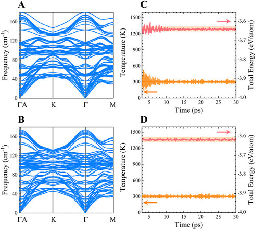
Figure 2. Phonon dispersion curves of stackings (A) GST-II and (B) GST-IV. Evolution of temperature (orange line) and total energy (red line) of atomic stackings (C) GST-II and (D) GST-IV as a function of time in AIMD simulations at 300 K.
Structural and electronic properties
Herein, we only investigated the atomic arrangements GST-I, GST-II, and GST-IV because the documented stacking GST-III can be considered as a mixture of GST-I and GST-II, as suggested in Ge2Sb2Te5[13], and thus its properties would obey Vegard’s law resembling the rules of mixtures[20,38,39]. After fully optimized structure relaxation, we found that the crystal symmetry has a slight difference that stacking GST-I retains the space group of R̅3m (No. 166) while GST-II and GST-IV adopt R3m (No. 160). As shown in Table 1, the calculated lattice parameters of stacking GST-I are in good agreement with experiments[22], suggesting the reliability of our calculations. In addition, the lattice constant c of stacking GST-IV (101.207 Å) is relatively smaller than those of GST-I (103.050 Å) and GST-II (103.546 Å), which results from the shorter Te-Te bond of the former, indicating that the atomic configurations have a certain effect on structural properties. Overall, the average length of the Te-Te bond in all the atomic stackings is appreciably longer than those of Ge-Te and Sb-Te bonds and is much larger than the sum of their covalent radii of 2.760 Å[40], manifesting the weak bonding nature between adjacent Te-Te layers.
Calculated lattice parameters (a and c) compared with available experiments (parentheses)[22]; average Ge-Te, Sb-Te, and Te-Te bond lengths; and electronic bandgaps (Eg) calculated using PBE functional and HSE06 functional (parentheses), respectively
Note that we first calculated the band structure including the effect of spin-orbital coupling (SOC), with stacking GST-I as an example [Supplementary Figure 4]. The resulting band curves with SOC are almost the same as those without SOC, indicating that the SOC has negligible influence on the electronic band structures and thus was ignored in our following calculations. Figure 3 illustrates the electronic band structures of stackings GST-I, GST-II, and GST-IV, where the orange and red lines denote the highest valence band (HVB) and the lowest conduction band (LCB), respectively. The corresponding calculations were performed on their primitive cell containing 17 atoms (i.e., Ge, 1; Sb, 6; Te, 10). Clearly, GST-I has a direct bandgap at the Z point [Figure 3A], whereas GST-II is an indirect semiconductor, as the valence band maximum (VBM) and the conduction band minimum (CBM) locate at different k-points along the Z-F line (the inset in Figure 3B). The estimated bandgaps using PBE functional are 0.20 and 0.05 eV for GST-I and GST-II [Table 1], respectively. Interestingly, GST-IV has no gap around the Fermi level (Ef) because the HVB marginally overlaps with the LCB around the G point [Figure 3C]. These results demonstrate that the atomic stackings have remarkable impacts on the electronic structures of Ge1Sb6Te10, thus affecting its electrical transport properties (as discussed below).
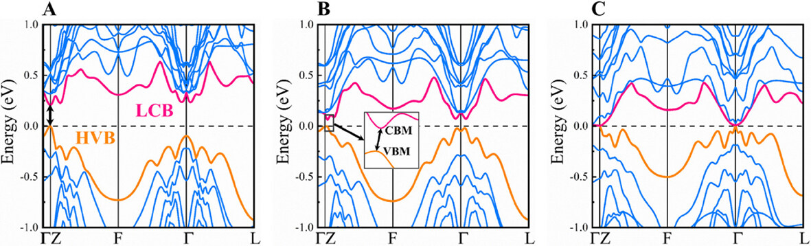
Figure 3. Electronic band structures of: (A) GST-I; (B) GST-II; and (C) GST-IV. The orange line is the highest valence band (HVB) and the red line represents the lowest conduction band (LCB). The inset of (B) is the zoomed in picture around the conduction band minimum (CBM) and valence band maximum (VBM). The Fermi level (Ef) is set to 0 eV.
Aiming to further improve the understanding of electronic structures, Figure 4 shows the projected density of states (PDOS) and pCOHP of stackings GST-I, GST-II, and GST-IV. For all the stackings, the PDOS pictures indicate that the bottom of the conduction bands mainly consists of Sb 5p and Te 5p orbitals, and the top of valence bands are primarily dominated by 5p electrons of Te atoms. It is also noticed that there are Ge 4s and Sb 5s peaks near the VBM, which hybridize with Te 5p orbitals, forming Ge 4s-Te 5p and Sb 5s-Te 5p antibonding states due to the negative values of -pCOHP. Moreover, Ge 4p and Sb 5p orbitals states are widely distributed in the energy range of -6 to 0 eV and strongly couple with Te 5p electrons, implying the covalent bonding characters of Ge-Te and Sb-Te bonds. Meanwhile, the pCOHP graphs show that Ge 4p-Te 5p and Sb 5p-Te 5p interactions within the same energy region exhibit positive -pCOHP values, substantiating their bonding states. Furthermore, no antibonding states were observed at Ef for these three configurations, manifesting their stable chemical bonding interactions.
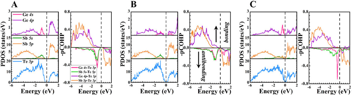
Figure 4. PDOS and pCOHP of stackings: (A) GST-I; (B) GST-II; and (C) GST-IV. The Ef is set to 0 eV.
Notably, the GGA-PBE method usually underestimates the electronic bandgaps of crystals, while the precise bandgap plays a significant role in obtaining more realistic electronic transport properties, especially at elevated temperatures[41]. Hence, the HSE06 functional was further employed to predict more accurate bandgaps, and the resulting bandgaps of stackings GST-I and GST-II increase to 0.45 and 0.16 eV [Table 1], respectively. However, GST-IV still has no bandgap, exhibiting semi-metallic characteristics. Since high-performance TE materials are generally narrow bandgap semiconductors[42], we only focused on studying the transport properties and TE performance of GST-I and GST-II. To give a qualitative description of electrical transport properties, Figure 5A and B displays the total DOS around conduction band (CB) and valence band (VB) edges of GST-I and GST-II. It is well known that a rapid change in DOS with energy is essential for obtaining a large Seebeck coefficient[43]. Clearly, the CB DOS for both stackings is considerably larger than their VB DOS throughout the energy range of 0-0.6 eV. In addition, both VB and CB DOS of stacking GST-I are much steeper than those of stacking GST-II. These results suggest that both stackings would exhibit higher n-type S than that of the p-type, and higher Seebeck coefficients of stacking GST-I under both n- and p-type dopings can be expected compared with GST-II.
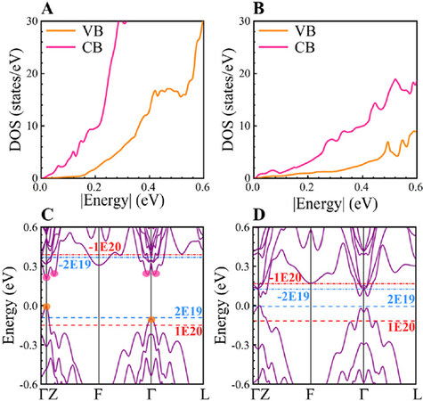
Figure 5. Total DOS of conduction bands (red line) and valence bands (orange line) around the respective CBMs and VBMs for stackings (A) GST-I and (B) GST-II. Electronic band structures of stackings (C) GST-I and (D) GST-II. The blue and red dashed lines indicate the Fermi level at the carrier concentrations of 2 × 10¹⁹ and 1 × 1020 cm-3, respectively. The positive and negative carrier concentrations represent the p- and n-type dopings, respectively. CBM: Conduction band minimum; VBM: valence band maximum.
Further, it is observed in Figure 5C that the second valence band maxima of GST-I located at the G-point is 0.1 eV lower in energy than VBM. This suggests that the hole transport in stacking GST-I is mainly dominated by the G pocket, and the Z pocket would participate in electrical transport when heavily doped, such as n = 1 × 1020 cm-3 (red dashed line in Figure 5C). However, the second conduction band valley located along the Z-F line is only about 0.02 eV from the CBM. Meanwhile, the third (on the G-L line) and fourth conduction band minima (on the G-F line) are slightly higher (~0.03 eV). In addition to the multi-conduction pocket electrons, multiband conduction is also observed, even at very low electron concentrations (e.g., n = -2 × 1019 cm-3, Figure 5C). Stacking GST-II has a similar band configuration [Figure 5D] to GST-I. As a result, the unique conduction band structures could greatly promote electrical conduction and thus are favorable for achieving high electrical conductivities and power factors.
Electrical transport properties
Noticeably, the thermal stability of GST-I and GST-II at 800 K was verified by performing AIMD simulations [Supplementary Figure 5]. Hence, both stackings are thermally stable in a wide temperature range of 300-800 K, and here we focus on the range from 300 to 710 K. In addition, the calculated temperature-dependent Seebeck coefficients of GST-I agree well with the experiments (see comparison details and Supplementary Figure 6A in the Supplementary Materials)[25], indicating the validity of our theoretical predictions. It is noted that layered GST compounds generally tend to show the p-type character. However, our previous work[44] made an extensive analysis to unravel the defect physics in these materials and suggests that it is quite likely to make n-type GST semiconductors by tuning the atomic chemical environments. Therefore, Figure 6A and E shows the Seebeck coefficients of GST-I and GST-II as a function of carrier concentration at different temperatures for both n- and p-types. At the same temperature, the absolute S value of stacking GST-I basically decreases with increasing carrier concentration, and, for the same carrier concentration, S increases with the temperature. GST-II exhibits peak S values for both p- and n-type dopings at higher temperatures (e.g., 520 and 710 K). It is also observed that GST-I has relatively larger Seebeck coefficients compared with GST-II. Meanwhile, the absolute n-type S values are significantly higher than those of the p-type for both stackings. For example, under the carrier concentration of 1 × 20 cm-3 and T = 710 K, the |S| values of stacking GST-I for p- and n-type dopings are 187 and 287 μV/K, respectively, while stacking GST-II has the values of 145 and 246 μV/K. Our calculated results are consistent with the above analysis of electronic properties.
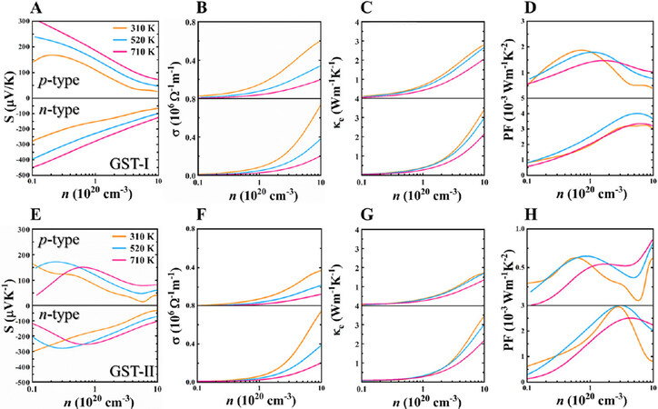
Figure 6. Electronic transport properties of (A-D) GST-I and (E-H) GST-II as a function of carrier concentration for p- and n-type dopings at different temperatures: (A, E) Seebeck coefficient S; (B, F) electrical conductivity σ; (C, G) electronic thermal conductivity κe; and (D, H) power factor PF.
In principle, using the BoltzTraP, the electrical conductivity can be estimated only if the electronic relaxation time (τ) is given. Here, τ is determined by the comparison between calculated σ/τ value and reported σ (see comparison details and Supplementary Figure 6B in the Supplementary Materials)[25], which has been widely employed in the evaluation of relaxation time for many materials[45-47]. The resulting τ values of stacking GST-I at different temperatures are shown in Supplementary Figure 6C, in which τ decreases with temperature (e.g., 20.1 fs at 310 K, 11.8 fs at 520 K, and 7.0 fs at 710 K). Given the fact that there are no experimental data for GST-II, the same relaxation time as stacking GST-I was used for better comparison. Figure 6B and F illustrates the changes of electrical conductivity with respect to carrier concentration at different temperatures. It is seen that electrical conductivity increases with carrier concentration at the same temperature, and, for the same doping level, σ decreases when increasing the temperature, exhibiting the metal-like behavior. In addition, the n-type σ for both stackings are larger than that of p-type, owing to their complex conduction bands discussed above. Interestingly, by comparing with stacking GST-II, GST-I with higher p-type Seebeck coefficient also possesses larger electrical conductivity for hole doping, suggesting its higher power factors and better p-type TE performance.
The electronic thermal conductivity was further calculated based on the Wiedemann-Franz law[48]: κe = LσT, where L is the Lorenz number. L of 1.5 × 10⁻⁸ WΩK-2 was selected as an empirical constant in our calculations, which has been used for many Te-based semiconductors[45,49,50]. As clearly shown in Figure 6C and G, κe gradually increases with increasing carrier concentration and decreases with the increase of temperature. The n-type κe is larger than that of p-type, owing to the larger n-type doped electrical conductivity. Furthermore, the power factor (PF) is derived from the Seebeck coefficients and electrical conductivities [Figure 6D and H]. At 310 K, the maximum n-type PF values are 3.24 and 2.95 mWm-1K-2 for GST-I and GST-II, respectively, while the p-type values are 1.88 and 0.63 mWm-1K-2. Apparently, both stackings exhibit significantly larger n-type PF than that of p-type due to the combination of higher n-type S and σ.
Phonon thermal transport properties
Lattice thermal conductivity is one of the critical factors that determine the TE performance of TE materials. Figure 7A presents temperature-dependent κl of GST-I and GST-II calculated by iteratively solving the phonon BTE. The κl of both stackings gradually decreases with increasing temperature, suggesting that the phonon-phonon scattering is primarily dominated by Umklapp processes. Moreover, they have similar κl values in the whole studied temperature range, although the former is marginally larger, indicating that stacking arrangement has no significant impact on phonon thermal transport performance. At 300 K, the predicted κl values are 0.86 (GST-I) and 0.78 Wm-1K-1 (GST-II) and decrease to 0.37 and 0.33 Wm-1K-1 at 710 K, respectively. To unravel the origin of the low κl, we calculated the group velocity of each phonon mode for stackings GST-I and GST-II. Figure 7B shows that the group velocities of most vibrations are in the range of 0-2500 m/s, indicating the slow phonon propagation in the crystal lattice. For a better understanding of the slow phonon transport, the longitudinal (vL), transverse (vT), and mean sound velocities (vm) were extracted from the elastic moduli (see the Supplementary Materials and Supplementary Table 2 for details) and bulk density ρ[51]:
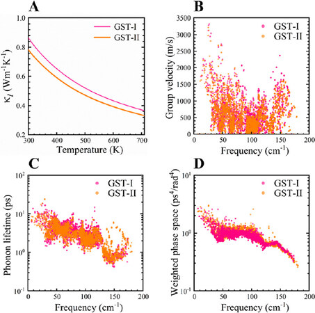
Figure 7. (A) Temperature dependence of lattice thermal conductivity; (B) group velocity; (C) room temperature phonon lifetime; and (D) weighted phase space of GST-I and GST-II.
As shown in Table 2, bulk and shear moduli of GST-I (B, 39.91 GPa; G, 25.66 GPa) are relatively higher than those of GST-II (B, 38.48 GPa; G, 24.25 GPa), leading to higher vL and vT of the former, thereby higher lattice thermal conductivity. Moreover, the vm values of GST-I and GST-II are 2.21 and 2.15 km/s, respectively, comparable to Bi2Te3-based alloys (~2.15 km/s)[52], further substantiating their slow phonon propagation.
Calculated bulk modulus B (GPa), shear modulus G (GPa), bulk density ρ (g/cm3), and sound velocities vL, vT, and vm (km/s) for stackings GST-I and GST-II, respectively
| Stacking | B | G | ρ | vL | vT | vm |
|---|---|---|---|---|---|---|
| GST-I | 39.91 | 25.66 | 6.47 | 3.39 | 1.99 | 2.21 |
| GST-II | 38.48 | 24.25 | 6.46 | 3.31 | 1.94 | 2.15 |
The phonon lifetime (τ), another essential parameter in evaluating the κl of crystals, was further calculated [Figure 7C]. Obviously, both stackings exhibit lower τ values at 300 K, which mainly stay within the range of 1-10 ps, similar to the region of τ for cubic methylammonium lead iodide MAPbI3 (κl < 1 Wm-1K-1 at room temperature)[53]. To better describe the τ, we averaged the phonon times of all vibration modes. By comparing with the average τ (3.22 ps) of stacking GST-I, GST-II gives a bit lower value of 2.98 ps, thereby leading to the slightly lower κl. In addition, the magnitude of the Grüneisen parameter (γ) is considered a good measure of lattice anharmonicity and able to reflect the strength of anharmonic phonon-phonon scattering[54]. Generally, a crystal with larger |γ| value indicates that it has higher degree of anharmonicity and stronger anharmonic scattering rate, giving rise to shorter phonon lifetime and lower lattice thermal conductivity. Therefore, the total Grüneisen parameter γtotal at 300 K was determined from a weighted sum of the mode contributions. It turns out that the γtotal is 1.40 for stacking GST-I and 1.15 for stacking GST-II. These γtotal values are comparable to, although slightly lower than, the value of PbTe (~1.45)[55], manifesting the appreciable phonon anharmonicity in both stackings of Ge1Sb6Te10 and thus short phonon lifetimes. Meanwhile, it should be expected that the larger γtotal of stacking GST-I gives a lower τ value than that of stacking GST-II. Nonetheless, our calculation results above demonstrate the opposite situation. To explain this, we calculated the weighted scattering phase space (W) [Figure 7D], which measures the number of three-phonon scattering channels for each vibration mode[56]. It shows that the W values of stacking GST-II are overall larger than those of GST-I, indicating that there are more three-phonon scattering processes of the former, which results in shorter phonon lifetimes. Collectively, it can be concluded that the low lattice thermal conductivity for both stackings of Ge1Sb6Te10 is well understood from the small phonon group velocity and short phonon lifetime.
Thermoelectric figure of merit
Using the obtained power factor and thermal conductivity, we estimated the ZT values of GST-I and GST-II, as shown in Figure 8. Apparently, the calculated ZT values of stacking GST-I are in excellent agreement with the experiments (Figure 8A, top)[25]. For both p- and n-type dopings, it is seen that the ZTmax of stackings GST-I and GST-II all rise with temperature, mainly due to the decrease in κe and κl. By modulating the carrier concentration to the optimal value of 5.3 × 1019 cm-3, the ZTmax of p-type GST-I reaches up to 1.36 at 710 K, exhibiting excellent p-type TE performance. This means that the low ZT values reported by experiments are mainly ascribed to the high hole concentration, and the TE performance can be appreciably improved through the reduction of carrier density using appropriate dopant. The PDOS above [Figure 4] demonstrates that the tops of valence bands are primarily dominated by 5p electrons of Te atoms and the Ge/Sb p orbitals have slight contributions. Therefore, it is possible to modulate the hole carrier concentration via Ge/Sb defect engineering without considerably influencing the valence band structure, thereby increasing the ZT value. For example, it is found that the homologous compound Ge2Sb2Te5 gives the maximal ZT value of 0.78 at 700 K by substituting the Ge sites with In, an about two-fold improvement compared with the undoped material system because the introduction of indium as a potentially donor-like dopant lowers the hole carriers density[8]. In addition, substituting with Cd leads to a considerable increase of the Seebeck coefficient of Ge1Sb2Te4 due to the significant reduction of hole concentration, and the power factor of Cd0.2Ge0.8Sb2Te4 exceeds that of undoped Ge1Sb2Te4 by a factor of about 2.5[12]. The ZTmax of p-type GST-II is 0.60 (n = 9.3 × 1019 cm-3) at 710 K [Figure 8B], overtly lower than that of stacking GST-I, which is attributed to its smaller Seebeck coefficient and electrical conductivity. It is very exciting that the peak ZT values for n-type GST-I and GST-II are as high as 2.23 and 1.91 at 710 K, respectively, with corresponding optimal carrier concentrations of 1.10 × 10²⁰ and 1.36 × 1020 cm-3. Such high ZTmax values are comparable to and even slightly larger than those of GeTe-based TE material Ge0.87Pb0.13Te + 3% Bi2Te3 (ZT = 1.9 at 773 K)[57]. Therefore, our results indicate that the layered Ge1Sb6Te10 will be of immense promise for medium-temperature TE applications.
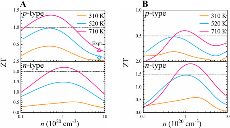
Figure 8. Dimensionless figure of merit ZT of stackings (A) GST-I and (B) GST-II as a function of carrier concentration for p- and n-type dopings at different temperatures. The dots in (A) represent the experimental results[25] at the concentration of 7.3 × 1020 cm-3.
Conclusions
By means of first-principle calculations combined with the Boltzmann transport theory, we carried out systematic investigations on the atomic stacking configurations, electronic structures, transport properties, and thermoelectric performance of layered Ge1Sb6Te10. Two novel atomic arrangements (GST-II and GST-IV) were predicted to be energetically, mechanically, dynamically, and thermally stable. GST-II and the experimentally known stacking GST-I were found to be semiconductors with narrow bandgaps of 0.45 and 0.16 eV, respectively, while GST-IV is a semimetal. Importantly, for the two semiconducting stacking configurations, high DOS of conduction band edge, multiple conduction pocket electrons, and multiband conduction give rise to large n-type Seebeck coefficients and electrical conductivities, thereby resulting in large power factors and better n-type TE performance. Moreover, both GST-I and GST-II exhibit low lattice thermal conductivities, 0.86 and 0.78 Wm-1K-1 at 300 K, and as low as 0.37 and 0.33 Wm-1K-1 at 710 K, owing to short phonon lifetimes and small phonon group velocities arising from the low elastic moduli. Consequently, the combination of high power factors and ultralow lattice thermal conductivities lead to the maximum ZT values of n-type GST-I and GST-II reaching up to 2.23 and 1.91 at 710 K, respectively, indicating the great promise of stacking polymorphic Ge1Sb6Te10 for TE application. We believe that our results provide great possibilities to discover novel functional materials from layered crystals and will stimulate further experimental research in the future.
Declarations
Authors’ contributionsContributed to conception and design of the study and performed data analysis and interpretation: Gan Y
Provided professional guidance: Zhou J, Sun Z
Availability of data and materialsSupplementary materials are available from the Journal of Materials Informatics or from the authors.
Financial support and sponsorshipThis work is supported by the National Key Research and Development Program of China (2017YFB0701700), the National Natural Science Foundation of China (51872017) and the high performance computing (HPC) resources at Beihang University.
Conflicts of interestAll authors declared that there are no conflicts of interest.
Ethical approval and consent to participateNot applicable.
Consent for publicationNot applicable.
Copyright© The Author(s) 2021.
REFERENCES
1. Raoux S, Wełnic W, Ielmini D. Phase change materials and their application to nonvolatile memories. Chem Rev 2010;110:240-67.
2. Zhang W, Mazzarello R, Wuttig M, Ma E. Designing crystallization in phase-change materials for universal memory and neuro-inspired computing. Nat Rev Mater 2019;4:150-68.
3. Zhang W, Thiess A, Zalden P, et al. Role of vacancies in metal-insulator transitions of crystalline phase-change materials. Nat Mater 2012;11:952-6.
4. Siegrist T, Jost P, Volker H, et al. Disorder-induced localization in crystalline phase-change materials. Nat Mater 2011;10:202-8.
5. Gan Y, Huang Y, Miao N, Zhou J, Sun Z. Novel IV-V-VI semiconductors with ultralow lattice thermal conductivity. J Mater Chem C 2021;9:4189-99.
6. Fahrnbauer F, Souchay D, Wagner G, Oeckler O. High thermoelectric figure of merit values of germanium antimony tellurides with kinetically stable cobalt germanide precipitates. J Am Chem Soc 2015;137:12633-8.
7. Rosenthal T, Schneider MN, Stiewe C, Döblinger M, Oeckler O. Real structure and thermoelectric properties of GeTe-rich germanium antimony tellurides. Chem Mater 2011;23:4349-56.
8. Hu P, Wei TR, Qiu P, et al. Largely enhanced Seebeck coefficient and thermoelectric performance by the distortion of electronic density of states in Ge2Sb2Te5. ACS Appl Mater Interfaces 2019;11:34046-52.
9. Wei T, Hu P, Chen H, et al. Quasi-two-dimensional GeSbTe compounds as promising thermoelectric materials with anisotropic transport properties. Appl Phys Lett 2019;114:053903.
10. Ibarra-hernández W, Raty J. Ab initio density functional theory study of the electronic, dynamic, and thermoelectric properties of the crystalline pseudobinary chalcogenide (GeTe)x/(Sb2Te3)(x=1,2,3). Phys Rev B 2018;97:245205.
11. Rosenthal T, Urban P, Nimmrich K, et al. Enhancing the thermoelectric properties of germanium antimony tellurides by substitution with selenium in compounds GenSb2(Te1-xSex)n+3(0 ≤ x ≤ 0.5; n ≥ 7). Chem Mater 2014;26:2567-78.
12. Welzmiller S, Fahrnbauer F, Hennersdorf F, et al. Increasing Seebeck coefficients and thermoelectric performance of Sn/Sb/Te and Ge/Sb/Te materials by Cd doping. Adv Electron Mater 2015;1:1500266.
13. Da Silva JLF, Walsh A, Lee H. Insights into the structure of the stable and metastable (GeTe)m(Sb2Te3)n compounds. Phys Rev B 2008;78.
14. Sun Z, Zhou J, Ahuja R. Structure of phase change materials for data storage. Phys Rev Lett 2006;96:055507.
15. Eom J, Yoon Y, Park C, et al. Global and local structures of the Ge-Sb-Te ternary alloy system for a phase-change memory device. Phys Rev B 2006;73.
16. Sa B, Miao N, Zhou J, Sun Z, Ahuja R. Ab initio study of the structure and chemical bonding of stable Ge(3)Sb(2)Te(6). Phys Chem Chem Phys 2010;12:1585-8.
17. Sa B, Zhou J, Song Z, Sun Z, Ahuja R. Pressure-induced topological insulating behavior in the ternary chalcogenide Ge2Sb2Te5. Phys Rev B 2011;84.
18. Kim J, Kim J, Jhi S. Prediction of topological insulating behavior in crystalline Ge-Sb-Te. Phys Rev B 2010;82.
19. Sa B, Zhou J, Ahuja R, Sun Z. First-principles investigations of electronic and mechanical properties for stable Ge2Sb2Te5 with van der Waals corrections. Comput Mater Sci 2014;82:66-9.
20. Sa B, Sun Z, Kaewmaraya T, Zhou J, Ahuja R. Structural and vibrational properties of layered data storage material: Ge2Sb2Te5. sci adv mater 2013;5:1493-7.
21. Campi D, Paulatto L, Fugallo G, Mauri F, Bernasconi M. First-principles calculation of lattice thermal conductivity in crystalline phase change materials: GeTe, Sb2Te3, and Ge2Sb2Te5. Phys Rev B 2017;95.
22. Shelimova LE, Karpinskii OG, Zemskov VS, Konstantinov PP. Structural and electrical properties of layered tetradymite-like compounds in the GeTe-Bi2Te3 and GeTe-Sb2Te3 systems. Inorg Mater 2000;36:235-42.
23. Matsunaga T, Kojima R, Yamada N, et al. Structural investigation of GeSb6Te10 and GeBi6Te10 intermetallic compounds in the chalcogenide homologous series. Acta Crystallogr B 2010;66:407-11.
24. Kosuga A, Nakai K, Matsuzawa M, et al. Enhanced thermoelectric performance of In-substituted GeSb6Te10 with homologous structure. APL Materials 2014;2:086102.
25. Kosuga A, Nakai K, Matsuzawa M, et al. Crystal structure, microstructure, and thermoelectric properties of GeSb6Te10 prepared by spark plasma sintering. J Alloys Compd 2015;618:463-8.
26. Hafner J. Ab-initio simulations of materials using VASP: Density-functional theory and beyond. J Comput Chem 2008;29:2044-78.
27. Wang G, Peng L, Li K, et al. ALKEMIE: An intelligent computational platform for accelerating materials discovery and design. Comput Mater Sci 2021;186:110064.
29. Perdew JP, Burke K, Ernzerhof M. Generalized gradient approximation made simple. Phys Rev Lett 1996;77:3865-8.
30. Grimme S. Semiempirical GGA-type density functional constructed with a long-range dispersion correction. J Comput Chem 2006;27:1787-99.
31. Paier J, Marsman M, Hummer K, Kresse G, Gerber IC, Angyán JG. Screened hybrid density functionals applied to solids. J Chem Phys 2006;124:154709.
32. Bylander DM, Kleinman L. Energy fluctuations induced by the Nosé thermostat. Phys Rev B Condens Matter 1992;46:13756-61.
33. Deringer VL, Tchougréeff AL, Dronskowski R. Crystal orbital Hamilton population (COHP) analysis as projected from plane-wave basis sets. J Phys Chem A 2011;115:5461-6.
34. Madsen GK, Singh DJ. BoltzTraP. A code for calculating band-structure dependent quantities. Comput Phys Commun 2006;175:67-71.
35. Li W, Carrete J, Katcho NA, Mingo N. ShengBTE: A solver of the Boltzmann transport equation for phonons. Comput Phys Commun 2014;185:1747-58.
36. Baroni S, de Gironcoli S, Dal Corso A, Giannozzi P. Phonons and related crystal properties from density-functional perturbation theory. Rev Mod Phys 2001;73:515-62.
37. Grimsditch M, Polian A, Brazhkin V, Balitskii D. Elastic constants of α-GeO2. J Appl Phys 1998;83:3018-20.
38. Cordero ZC, Schuh CA. Phase strength effects on chemical mixing in extensively deformed alloys. Acta Materialia 2015;82:123-36.
40. Cordero B, Gómez V, Platero-Prats AE, et al. Covalent radii revisited. Dalton Trans 2008:2832-8.
41. Mishra SK, Satpathy S, Jepsen O. Electronic structure and thermoelectric properties of bismuth telluride and bismuth selenide. J Phys: Condens Matter 1997;9:461-70.
42. Gorai P, Stevanović V, Toberer ES. Computationally guided discovery of thermoelectric materials. Nat Rev Mater 2017;2.
43. Heremans JP, Jovovic V, Toberer ES, et al. Enhancement of thermoelectric efficiency in PbTe by distortion of the electronic density of states. Science 2008;321:554-7.
44. Sun Z, Pan Y, Zhou J, Sa B, Ahuja R. Origin of p-type conductivity in layered nGeTe·mSb2Te3 chalcogenide semiconductors. Phys Rev B 2011;83:113201.
45. Li Z, Miao N, Zhou J, Sun Z, Liu Z, Xu H. High thermoelectric performance of few-quintuple Sb2Te3 nanofilms. Nano Energy 2018;43:285-90.
46. Einhorn M, Williamson BAD, Scanlon DO. Computational prediction of the thermoelectric performance of LaZnOPn (Pn = P, As). J Mater Chem A 2020;8:7914-24.
47. Gandi AN, Schwingenschlögl U. WS2 as an excellent high-temperature thermoelectric material. Chem Mater 2014;26:6628-37.
48. Jonson M, Mahan GD. Mott’s formula for the thermopower and the Wiedemann-Franz law. Phys Rev B 1980;21:4223-9.
49. Kim SI, Lee KH, Mun HA, et al. Thermoelectrics. Dense dislocation arrays embedded in grain boundaries for high-performance bulk thermoelectrics. Science 2015;348:109-14.
50. Li Z, Han S, Pan Y, et al. Origin of high thermoelectric performance with a wide range of compositions for BixSb2-xTe3 single quintuple layers. Phys Chem Chem Phys 2019;21:1315-23.
51. Anderson OL. A simplified method for calculating the debye temperature from elastic constants. J Phys Condens Matter 1963;24:909-17.
52. Poudel B, Hao Q, Ma Y, et al. High-thermoelectric performance of nanostructured bismuth antimony telluride bulk alloys. Science 2008;320:634-8.
53. Wang M, Lin S. Anisotropic and ultralow phonon thermal transport in organic-inorganic hybrid perovskites: atomistic insights into solar cell thermal management and thermoelectric energy conversion efficiency. Adv Funct Mater 2016;26:5297-306.
54. Morelli DT, Jovovic V, Heremans JP. Intrinsically minimal thermal conductivity in cubic I-V-VI2 semiconductors. Phys Rev Lett 2008;101:035901.
55. Roufosse M, Klemens PG. Thermal conductivity of complex dielectric crystals. Phys Rev B 1973;7:5379-86.
56. Li W, Mingo N. Ultralow lattice thermal conductivity of the fully filled skutterudite YbFe4Sb12 due to the flat avoided-crossing filler modes. Phys Rev B 2015;91:144304.
Cite This Article
Export citation file: BibTeX | RIS
OAE Style
Gan Y, Zhou J, Sun Z. Prediction of the atomic structure and thermoelectric performance for semiconducting Ge1Sb6Te10 from DFT calculations. J Mater Inf 2021;1:2. http://dx.doi.org/10.20517/jmi.2021.03
AMA Style
Gan Y, Zhou J, Sun Z. Prediction of the atomic structure and thermoelectric performance for semiconducting Ge1Sb6Te10 from DFT calculations. Journal of Materials Informatics. 2021; 1(1): 2. http://dx.doi.org/10.20517/jmi.2021.03
Chicago/Turabian Style
Gan, Yu, Jian Zhou, Zhimei Sun. 2021. "Prediction of the atomic structure and thermoelectric performance for semiconducting Ge1Sb6Te10 from DFT calculations" Journal of Materials Informatics. 1, no.1: 2. http://dx.doi.org/10.20517/jmi.2021.03
ACS Style
Gan, Y.; Zhou J.; Sun Z. Prediction of the atomic structure and thermoelectric performance for semiconducting Ge1Sb6Te10 from DFT calculations. J. Mater. Inf. 2021, 1, 2. http://dx.doi.org/10.20517/jmi.2021.03
About This Article
Copyright

Data & Comments
Data
0

 Cite This Article 18 clicks

 Like This Article 31
likes
Like This Article 31
likes


Comments
Comments must be written in English. Spam, offensive content, impersonation, and private information will not be permitted. If any comment is reported and identified as inappropriate content by OAE staff, the comment will be removed without notice. If you have any queries or need any help, please contact us at support@oaepublish.com.